EDA · 2026
Sirkit: from a circuit description to checked fabrication files
Sirkit takes a plain-language description of a small circuit, builds a netlist from real KiCad library parts, places and routes a two-layer board, and writes Gerber and drill files only after a chain of deterministic checks passes. A language model drafts the circuit. Everything after that is ordinary EDA code whose job is to prove the board is the circuit that was drafted, or refuse to continue.
- Status
- Runs end to end. JLCPCB fabricated the generated board, and it works in hardware
- My part
- Architecture and specifications for the board, routing and manufacturing stages, and the verification gates between them. The first prompt-to-schematic version was a collaboration with Shantanu Todmal.
- Stack
- TypeScript and Next.js, Postgres, KiCad symbol and footprint libraries, FreeRouting 2.2.4 (Specctra DSN/SES), ngspice
- Code
- Private repository
What it does
The pipeline has one stage that can make things up, so the design question was where to put the walls. The language model plans the circuit, searches a catalog of parts and proposes connections. What comes out is a JSON netlist that refers to catalog parts by ID. From there on, each stage either produces something it can check against the previous stage or stops.
Parts the model can’t invent
Every part in the catalog is backed by a parsed symbol and footprint from the official KiCad libraries, with content hashes, the package it claims to be, and an explicit map from each symbol pin to its footprint pad(s). If the model asks for a part, a pin or a value that isn’t in the catalog, the build fails instead of guessing at a near neighbor. For the demo that catalog was 21 seeded parts, which is narrow on purpose: anything outside it fails closed.
ERC findings from stage 3 go back to the model as feedback, at most twice. That bound is a weak spot: after two rejections the design is accepted with its findings attached. The stages after it are hard stops.
Keeping the schematic and the board the same circuit
Most of the work went into identity. A net on the board has to be the same net as in the schematic even after parts are placed, swapped, routed and saved to and loaded from the database. Net IDs are derived from the canonical set of endpoints they connect, so two representations of the same connectivity get the same ID. The parity check walks every intended endpoint, finds the footprint pad it maps to, and compares the net the board actually assigns with the one the schematic intended:
const netMembershipMismatches = intendedEndpoints.flatMap((endpointKey) => {
  const expected = expectedNetByEndpoint.get(endpointKey);
  const assigned = assignedNetByEndpoint.get(endpointKey);
  const intentional = intentionalNoConnects.includes(endpointKey);
  if ((!expected && intentional) || expected === assigned) return [];
  return [{ endpointKey, ...(expected ? { intendedStableNetId: expected } : {}),
                         ...(assigned ? { assignedStableNetId: assigned } : {}) }];
}).sort((a, b) => compareCodePoints(a.endpointKey, b.endpointKey));
Placement and routing
The board outline is sized from the parts’ courtyard area. Placement is force-directed: nets pull connected parts together, parts repel each other with a 1/d² force, and a boundary force keeps them on the board. Each part is tried in four orientations, and overlaps are resolved by snapping to a grid and searching outward in a spiral. The random seed is fixed, so the same netlist gives the same placement.
Routing is done by FreeRouting, run as a separate process. Sirkit writes the board as a Specctra DSN file, including net classes (Default, Power, HighCurrent) with their own track widths, clearances and via types, and reads the routed session file back with strict error codes. Copper that was already locked is preserved.
for (const classId of ["Default", "Power", "HighCurrent"] as DsnClassId[]) {
  const nets = dsn.networks.filter((net) => net.classRef === classId);
  if (nets.length === 0) continue;
  const rule =
    dsn.rules.find((r) => r.scope.kind === "class" && r.scope.classId === classId) ??
    dsn.rules.find((r) => r.scope.kind === "default");
  const viaName = rule?.viaCandidateName ?? VIA_NAME_BY_CLASS[classId];
  L.push(`    (class ${classId} ${nets.map((net) => q(net.name)).join(" ")}`);
  L.push(`      (circuit (use_via ${q(viaName)}))`);
  if (rule) L.push(`      (rule (width ${n(rule.widthNm)}) (clearance ${n(rule.clearanceNm)}))`);
  ...
}
Design rules from the fabricator
The DRC is Sirkit’s own: clearance, track width, via size and drill, annular ring, hole-to-hole spacing, board-edge clearance, courtyards, silk-to-pad spacing, and unconnected or shorted nets. Rules merge from the default to the net class to the individual net. The profile used for two-layer boards comes from JLCPCB’s published capabilities:
| Rule | Default | Power | HighCurrent |
|---|---|---|---|
| Clearance | 0.127 mm | 0.2 mm | 0.3 mm |
| Minimum track width | 0.127 mm | 0.4 mm | 1.0 mm |
| Via (outer / drill) | 0.6 / 0.3 mm | ||
| Annular ring (via / plated hole) | 0.15 / 0.25 mm | ||
| Hole to hole · board edge | 0.5 · 0.3 mm |
KiCad’s own DRC (kicad-cli pcb drc) is used only as an outside reference in an optional test that loads Sirkit’s exported board into KiCad and compares error counts.
Writing Gerbers without KiCad
Stage 8 compiles the board directly to Gerber X2 (with file, aperture and object attributes), an Excellon drill file and a job file, then reads every layer back with an independent parser and compares the geometry with the board model before anything is zipped. The archive is deterministic: releasing the same board twice produces byte-identical files, and a test corrupts one coordinate after writing to make sure the parse-back catches it.
function emitPrimitive(lines: string[], primitive: MirPrimitive, aperture: ApertureSpec): void {
  emitObjectAttributes(lines, primitive.attributes);
  lines.push(`D${aperture.code}*`);
  if (primitive.kind === "stroke") {
    lines.push(`${xy(primitive.start)}D02*`);     // move
    lines.push(`${xy(primitive.end)}D01*`);       // draw
  } else if (primitive.kind === "flash") {
    lines.push(`${xy(primitive.at)}D03*`);        // flash a pad
  } else {
    lines.push(`%TA.AperFunction,${primitive.apertureFunction}*%`);
    lines.push("%LPD*%");                          // dark polarity: copper
    emitRing(lines, primitive.outer);
    if (primitive.holes.length > 0) {
      lines.push("%LPC*%");                        // clear polarity: cut holes
      for (const hole of primitive.holes) emitRing(lines, hole);
      lines.push("%LPD*%");
    }
    lines.push("%TD.AperFunction*%");
  }
  lines.push("%TD*%");
}
Determinism took more work than the format. Aperture codes were originally derived from a JSON string of the pad shape, which depends on property order. A board that had been round-tripped through Postgres’s jsonb came back with sorted keys, so its content digest matched while its aperture numbering, and therefore its copper bytes, did not. Keys are now canonical, and a regression test reproduces the original case.
Result: one prompt to a fabrication package
The acceptance prompt for the demo, verbatim:
Design a hand-solderable 5 V LED blinker using a 555 timer in astable mode at approximately 1 to 1.5 Hz. Use an SOIC-8 timer, 0805 resistors and capacitors, an 0805 LED, and a two-pin 2.54 mm through-hole power header. Include supply decoupling and a control-pin bypass capacitor. Make a compact two-layer PCB suitable for JLCPCB fabrication. […]
No netlist, part list or values were supplied. The accepted run chose RA = 22 kΩ, RB = 47 kΩ and C = 10 µF. A separate script, which shares no code with Sirkit, recognized the astable topology from the generated netlist and computed 1.24 Hz nominal (1.12–1.39 Hz across resistor and capacitor tolerance) at 59.5 % duty. That is a closed-form check, not a SPICE simulation: the part catalog has no NE555 model, and I didn’t want a made-up one.
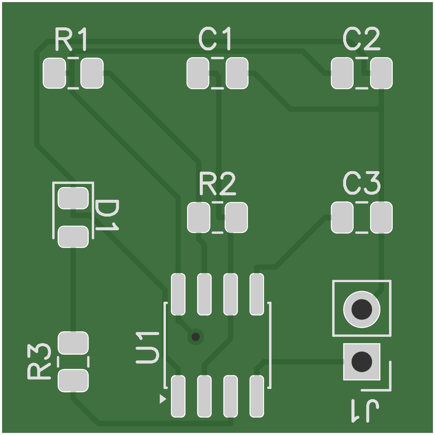
The board passed with no unrouted connections, no shorts and no blocking DRC errors. Qualification, including the real FreeRouting run, took 19.9 s. After fixing the defects the first live runs exposed, eight runs in a row completed end to end.
One of those fixes was an electrical mistake rather than a software one. An earlier run picked a 1 kΩ LED resistor. That sounds fine from a 5 V rail, but a bipolar 555’s output only gets to about VCC − 1.7 V, so the LED would have seen about 1.4 mA typical and 0.9 mA at worst-case forward voltage: too dim to show anything. The design guidance now sizes LED resistors from the loaded output-high voltage, and the accepted run used 330 Ω (about 4.2 mA).
In hardware
JLCPCB fabricated the board from Sirkit’s output, and I’ve validated it in hardware: it works. That is the one check none of the gates above can make. They show the Gerbers are consistent with the design Sirkit drafted; only a real board shows the design itself was right.
What isn’t done
- The verified release is bare-board only. Assembly files (BOM and pick-and-place) are left out until part sourcing is checked as carefully as footprints.
- The KiCad schematic export is flat and one-way. Hierarchical sheets exist in a newer schematic compiler that isn’t on this path yet.
- Four-layer routing is implemented but has only been tested on a small fixture.
- The part catalog is small, and the core PCB test suites run locally rather than in CI; only the prompt-to-Gerber replay and the manufacturing tests run on every push.