FPGA CPU Datapath Design
Custom multicycle MIPS processor on an FPGA with a full verification suite
Designed and implemented a multicycle MIPS CPU datapath on a Xilinx FPGA using Verilog. Developed control logic, ALU operations, and memory interfacing to support a subset of MIPS instructions. Created a comprehensive verification suite with over 50 test cases to ensure functional correctness and performance optimization.
Implemented full datapath supporting 20+ MIPS instructions
Developed control unit with state machine for multicycle execution
Created extensive testbench with directed and random tests
Achieved timing closure at 100MHz clock frequency
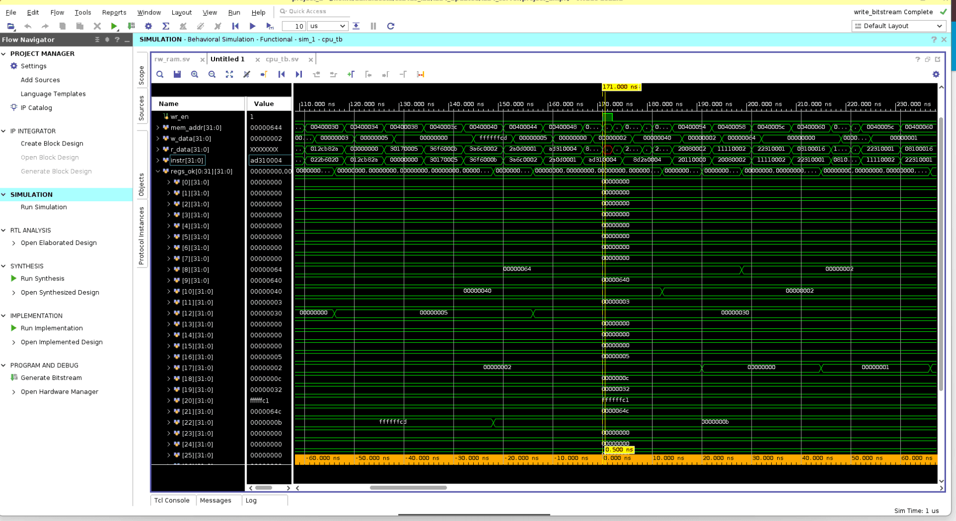
Prove it before you trust it
Simulation waveforms from the verification suite. I built 50+ directed and random test cases to prove the datapath actually executes each instruction correctly before trusting it on hardware.
The multicycle datapath
The MIPS datapath I designed in Verilog — ALU, control logic, and memory interfacing supporting 20+ instructions on a Xilinx FPGA.
Sequencing and timing closure
The multicycle control state machine and clocking. Reaching timing closure at 100 MHz meant the control unit had to sequence each instruction across exactly the right number of cycles.
Want the full story?
Happy to talk through any of the engineering decisions, trade-offs, or what broke along the way.